Recently, a friend of mine, who started to be interested in electronics and circuit engineering, asked me to give him some practical advice on the development of electronic devices. This question prompted us to sit down and formulate at least a small list of such recommendations. This is how this article turned out.
Table of Contents
Introduction
The article is a list of ten basic design rules that are relevant in the development of a wide range of devices. In article I intentionally do not mention the moments concerning designing of printed-circuit boards is a subject for separate conversation.
This list of rules does not claim to completeness and absolute truth, it contains only my experience of working out of electronic devices.
1. Install the capacitors on the chip supply
The presence of power supply capacitors is a prerequisite for normal operation of any chip. They provide the pulse current that the chip consumes when switching internal transistors. If there is no capacitor in close proximity to the chip, due to inductance of PCB tracks the current front can be swamped and the required speed of its rise will not be provided.
It may well be that the chip will not work at all, such cases occur. Due to this feature, capacitors with low ESR and ESL (equivalent in series resistance and equivalent in series inductance) should be chosen. In the overwhelming majority of cases, ceramic capacitors perform well, and if a large capacity is required, tantalum capacitors.
The number of capacitors per chip must be at least the number of power legs of the chip. That is, if the chip has 10 power leads, then it is necessary to put not less than 10 capacitors on only one of this chip, and to place these capacitors on the printed circuit board it is necessary as close to power leads as possible. Often manufacturers recommend to install one more additional capacitor of higher rating common for all power leads of the chip.
The following figure shows an example from the STM32F103 microcontroller documentation: as you can see, in addition to 5 0.1 µF capacitors at the VDD outputs, the manufacturer also recommends installing one common 4.7 µF capacitor.
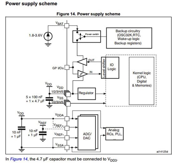
The choice of capacitor capacity deserves special attention. In most cases you will not be mistaken if you choose a capacitance of 0.1 μF. However, do not be lazy to look at the chip documentation on this issue: there may also be subtleties.
For example, RF microcircuits often require a capacitor with a smaller capacity. Below is a picture from the LT5560 mixer chip documentation. As you can see from the picture, the manufacturer advises to use capacitors 1 μF and 1 nF.
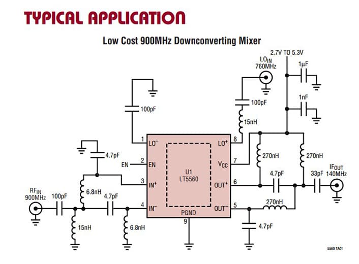
There may also be deviations in the other direction: for example, for a 4G module, the WP7502 requires the installation of a capacitor with a capacity of up to 1500 UF near the power supply terminals:
In general, it is always better to specify the values of the required capacitors in the documentation for a specific chip.
2. Consider the maximum parameters of the components
Unfortunately, it is not so rare to find circuits where the resistor in the 0402 case is in the 220 V circuit or something similar. You can’t do that!
Before installing any (absolutely any) component on the circuit, you must make sure that under no circumstances are the maximum permissible parameters for current, voltage, and power dissipation for this component exceeded.
All calculations must be made for the worst operating conditions (in particular, for the maximum possible voltage on the circuit), and the limit parameters should be found in the documentation for a specific component.
Let’s look at a simple example with a resistor. Let’s say we have calculated the circuit and we need to provide a resistance of 25 kOhm, and the maximum allowable voltage in this circuit is 100 V. What resistor will we put in the circuit? Open the documentation for RC series resistors from Bourns and see the main limit parameters:
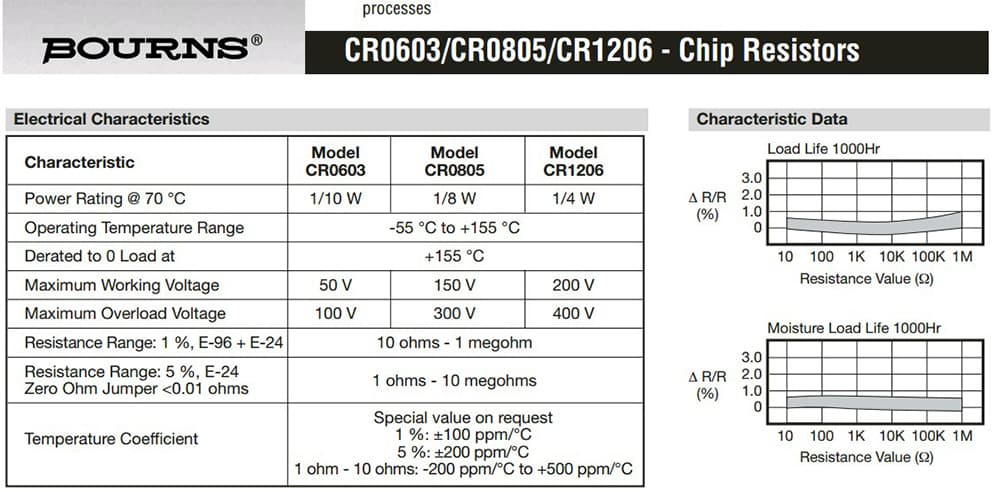
In circuits with a voltage of 100 V, resistors of the CR0805 or CR1206 series can work. CR0603 cannot be put there. What about power dissipation? As the school physics course says, for a DC circuit, it is calculated by the formula:

None of the resistors shown in the table can withstand this power, but we can connect several of them in parallel: 4 pieces of CR0805 or 2 pieces of CR1206. Just do not forget that when the resistors are connected in parallel, their equivalent resistance decreases.
For example, we can take 4 PCs CR0805-JW-104ELF (100 kOhm): connecting them in parallel, we get just 25 kOhm. For critical applications, you can further reduce the load on each of the resistors by connecting 6 pieces in parallel instead of 4 pieces.
The maximum permissible current for the RC series resistor is 2 A, and it will not be exceeded here, this is easily checked by the Ohm’s law. Moreover, this parameter is mainly relevant for resistors with a small resistance, for the rest you will run into excess power much faster.
And how to choose capacitors? After determining the type of capacitor used (ceramics, tantalum, film, electrolyte, etc.), it is necessary to provide a voltage margin of at least 25-30%. If possible, it is better to take the stock twice for critical applications.
In some cases, in addition to the voltage, it is also necessary to take into account the pulse current through the capacitor. This parameter is very often forgotten, although the current overload of the capacitor in the circuits of some switching power source will not end well. Considered example. Let’s say we have calculated our switching power supply and determined that it is:
- Operates at a frequency of 100 kHz.
- The voltage output of the circuit is 30 V.
3.a capacitor with a capacity of at least 100 UF is Required.
4.a pulse current of 2 A (current value) will flow through it.
The capacitance and voltage of the capacitor are large enough, so the use of an electrolytic capacitor is justified. For example, EEH-ZA capacitors from Panasonic are suitable.
Open the documentation for them:
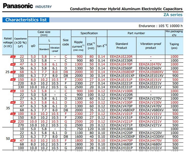
At first glance, it seems that 35 V is more than 30 V, and this capacitor should suit us. However, in this case, the supply will be only 5 V, which is very small. The correct solution is to choose a 50 V capacitor.
Look further: we have a 50 V capacitor with the required capacity of 100 UF. We could take it, but its maximum current is equal to our expected 2 A (for a frequency of 100 kHz), that is, again, there will be no margin for this parameter.
Therefore, it is correct to take two capacitors at 68 UF 50 V and connect them in parallel. Thus, we will get a total capacity of 132 UF, a maximum voltage of 50 V and a maximum pulse current of 3.6 A. This system will be reliable and will work for a long time.
Similarly, chokes, transistors, and any other components are selected. You should always remember about their maximum parameters and take components with a margin of at least 25-30%.
To the limit parameters can also be attributed to the temperature. There are three main temperature groups:
- Commercial (0 ℃…+70 ℃)
- Industrial (-40 ℃…+85 ℃)
- Military (-55 ℃…+125 ℃)
This division is not absolute, there are also all sorts of extended sub-ranges. But one thing is important – all (absolutely all) components on your circuit must fall within the temperature range specified in the technical task. In other words, when designing a circuit, you should always keep in mind the required operating temperature range and select components according to it. The operating temperature ranges (as well as the limit temperature ranges) are always given in the documentation.
3. Protect yourself from static
An electrostatic discharge can burn out the ports of a chip worth thousands of dollars in a fraction of a second. For this reason, you should always keep it in mind and take measures to protect your devices. In General, the topic of protection from static electricity is quite extensive and in itself deserves a separate article. Within this framework, we will try to briefly consider the basic rules that I have developed for myself:
- all interface connectors (USB, UART, RS-232, etc.) that the user will contact later must be protected from static electricity.
- all buttons that the user clicks on must be protected from static, provided that they are wound up on sensitive chips..
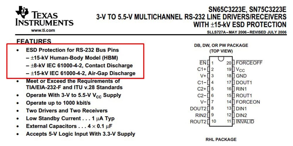
- if the terminal driver already has built-in protection against static, and if the operation of the product does not involve harsh conditions, you can not put additional protection. An example is the RS-232 sn65c3223 Converter, which already has built-in static protection.
- If the product is intended to be used in harsh conditions, the built-in protection may not be sufficient and you will need to add additional external elements.
Protect whether from static intra unit connectors – it depends on the culture of your production. If the installation takes place in special rooms with anti – static furniture and floor coverings, and all installers use anti-static bracelets-this may not be necessary. Under other conditions, protection will also not be superfluous.
The following requirements apply to static protection elements:
- They must withstand the specified energy of an electrostatic discharge.
- They must be rated for the appropriate operating voltage. It makes little sense to put a protective diode at 15 V in a circuit whose maximum allowable voltage is 3.6 V.
- They must have a small parasitic capacity (for high – speed circuits-maximum picofarad units). If you put some powerful protective diode (which will almost certainly have a large capacity) in the USB 3.0 circuit, then just block the signal fronts and nothing will work.
- They should have small leakage currents. The typical value is units per.
- on the printed circuit Board, they must be located in close proximity to the connector, and the path of the printed circuit Board must pass strictly “connector output -> security element-> protected component”.
- After the protective diode and before the chip, it is useful to put the resistor in units-tens of Ohms, if this is acceptable. This resistor will help to dissipate a possible surge of voltage on the protective diode during a strong discharge.
What exactly should use as static protection? Now there is a fairly rich selection:
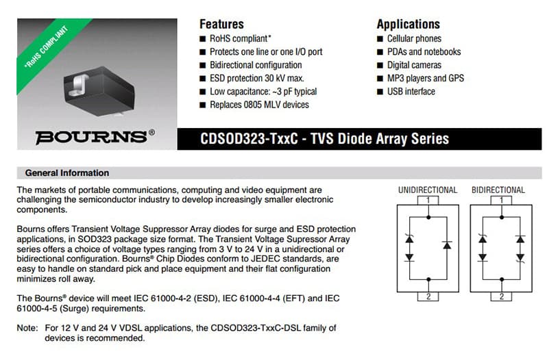
- Protective diodes with a fixed voltage level. An example is the cdsos323 diode. there Are both unidirectional and bidirectional versions of such protective diodes:
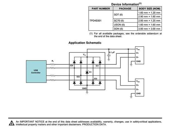
2.Protective diodes with a voltage level determined by the power source. An example is the TPD4E001 diode Assembly: the operating voltage range of Vcc is from 0.9 to 5.5 volts.
Next to such diodes, it is recommended to place a small-capacity capacitor that is powered on.
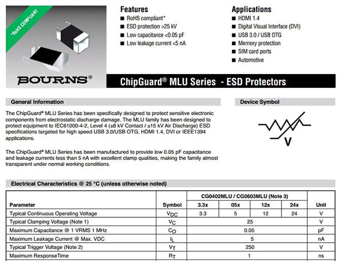
3. The varistors. There are special types designed to protect against static. An example is CG0402. Thanks to the ultra-small capacity of hundredths of a picofarad, they can be used in high-speed devices such as USB 3.0 or HDMI:
Do not use Zener diodes for static protection! They are meant for something else.
in particularly severe cases, you may need to use gas dischargers, but this is not really about static 🙂
4. Safety is first
The main rule of the developer should be “Create devices that are safe for others”.
In this section, I will look at some of the most common things that can be dangerous:
- As soon as the voltage in your circuit exceeds 30 V (and when operating in high humidity conditions of 12 V), start thinking about how to protect the user from them.
- When working with 220 V networks, be extremely careful. Provide reliable galvanic isolation between primary and secondary circuits. Cutouts in the printed circuit Board will be quite useful here. The user’s contact with the primary chain must be completely excluded!
- If you are designing devices that are powered by a network, understand what type x and Y capacitors are, apply them in the appropriate places, and never replace them with ordinary film or ceramics.
- When working with high voltages, the metal housing of your equipment must be grounded.
- Fuses and other protection devices are quite useful things.
- Do not rely on microcontrollers to set up protective shutdown circuits, as they tend to freeze. Always duplicate such important chains with some oak logic.
- Provide discharge circuits for high-voltage capacitors. After switching off the device, they should be discharged as quickly as possible.
Medical equipment is a separate story. Don’t start developing it without getting familiar with all the security requirements that apply to this type of hardware
More information on the topic of security can be obtained in the GOST and other standards.
5. Put protection from the fool
If you think that the user will not confuse the Pinout of your power connector or will not supply 27 V instead of 12 V, then you are mistaken, this will happen sooner or later. This can be avoided if your equipment is powered via a standard connector, but in any other case, I recommend protecting the input power circuits from user errors.
Of course, little will save you from a nuclear explosion or from direct connection to a 10 kV substation, but the basic elements of protection must be present. In this article, I will very briefly consider two types of protection: from reverse polarity and from increased input voltage.
There are already quite a lot of schemes for protection against reverse polarity, but in my practice I widely use two of them: with the use of a diode and with the use of a field-effect transistor.
The diagram of protection against reverse polarity using a diode is shown in the figure:
The advantage of this scheme is its extreme simplicity, but it has a big disadvantage: the VD1 diode can get very hot. The power allocated on it can be roughly estimated by multiplying 0.4…0.8 (the voltage drop on the open diode) by the current consumption of the circuit.
For accurate calculation, you can use the VAC of the diode, which is always available in the documentation for it. But it is so obvious that at a current of 1 A, several tenths of a watt will be allocated on the diode, which will not only be wasted, but, in the absence of a heat sink, will most likely quickly kill the diode (especially if it is in a small case). Therefore, this protection scheme can be used only if the current consumed does not exceed units-tens of milliamps.
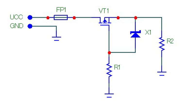
For more powerful circuits, it is better to use the protection circuit on the field-effect transistor, it is shown in the figure:
In this article, I will not tell you how this scheme works and how to count it, it has already been written about a lot of places, and the interested reader will not have problems finding information. Therefore, we will immediately proceed to overvoltage protection schemes.
To protect against overvoltage, there are at least two approaches: installing any electronic fuses (hotswaps, power controllers) at the input of the circuit, or installing voltage limiters. Of course, you can combine these two approaches in one scheme.
Electronic fuse chips come with a variety of functions: they can be able to monitor high voltage, low voltage, provide protection for current, temperature, power, provide a smooth increase in current, and much more. An example of a good electronic fuse can serve as a chip TPS1663, the typical circuit of which is shown below:
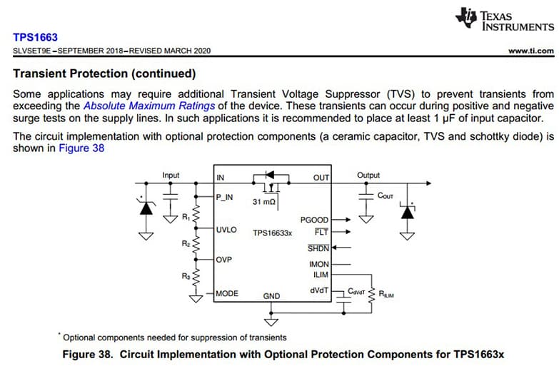
This chip provides protection against overvoltage, but it itself has a maximum allowable voltage of 67 volts. How to protect yourself in this case? Unfortunately, you will not be able to increase protection indefinitely, and in this case there is only one option: to allow something cheap to burn in the scheme and break the chain, saving all the valuable stuffing of the scheme. And then we move smoothly to the voltage limiters.
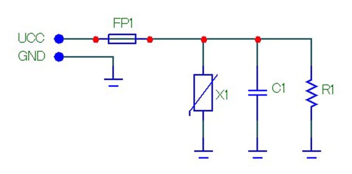
The voltage limiter can be a varistor, a protective diode (TVS), or even a gas discharger. Talking about the pros and cons of each would be drawn to a separate article, so this article will not be considered. It makes sense to use voltage limiters in conjunction with a fuse: in this approach, a varistor or protective diode limits the voltage by passing a large current through it, which causes the fuse to burn and break the circuit.
If the circumstances are not very successful, the limiter itself can also burn, but the valuable chips on the Board must be saved and, which is also very important, a possible fire is prevented. The simplest protection scheme for a device using a varistor is shown below:
We have reviewed the main schemes for protecting the Board from power overshoot and overvoltage. The developer must choose the optimal combination of protection schemes based on the requirements for reliability, the probability of user error, space on the printed circuit Board, and the cost of the product. As a conclusion for this section, I will give a fragment of the input stage scheme implemented in one of my recent developments.
This scheme provides a full range of protections: protection against reverse polarity on the field-effect transistor, protection against low and high voltage, as well as current protection on the tps1663 chip, and to top it all, protection with a varistor and a fuse.
6. Practice a systematic approach to development
A very common mistake of novice developers is to draw a diagram, separate the Board (maybe even make it), and only then think about the device case. And here the most interesting thing begins: it seems that there is a great case for the device on sale, it would almost fit… if the Board was a millimeter or two shorter. And the next standard size of the case is already one and a half times larger, but you have to take it, because the alternative-making the case to order-is too expensive.
As a result, we have an unnecessarily large case, in which a small printed handkerchief is dangling. But this could have been avoided if the issue of working out the hardware case was not left for later, but solved simultaneously with the development of the printed circuit Board.
When a complex device with a custom case is being developed, then high-quality development can’t happen without a close collaboration of the designer, circuit engineer and topologist (sometimes, however, it is the same person :)). It is important to understand that this work occurs simultaneously: circuitry draws a diagram and sends it to the topologist, the designer at this time determines the dimensions of the printed circuit boards depending on design of the product, and also provides various restrictions on the height of the components and restricted areas, topologist makes a preliminary alignment of the components on the PCB and passes it to the constructor for integration in the overall 3D model, all circuitry negotiates and, when necessary, responds to the wishes of the type “here would choke to pick up a couple of millimeters lower”.
But an integrated approach to development is not limited to design.
If the product involves writing built-in software, it is necessary to interact with the circuit engineer and programmers at the stage of developing the block diagram of the future device. This is necessary both for planning the development time, and for determining the possibility of software implementation of embedded circuit solutions.
Unfortunately, the lack of circuitry knowledge of software development, some inherent in the solution scheme can be in principle feasible from the point of view of writing software, and it turns out it’s only after the manufacture of printed circuit boards. Therefore, in order to avoid such a sad scenario, it is worth considering and coordinating all the issues that are fundamental from the point of view of SOFTWARE with those who will then write this SOFTWARE.
In addition, when talking about an integrated approach, it is impossible not to mention such an important point as the organization of future production. Already at the stage of drawing the diagram, you need to think about how this Board will be produced later, how to debug it, check it, and test it. Right now, you need to set up control points for measuring the voltage of power sources, think about jobs, about all sorts of cables and where to connect them, about the verification procedure.
It may very well be that to test your Board in mass production, you will need special equipment – its development (at least in draft form) should be started in parallel with the Board being tested, because these are two interconnected devices. In General, take a comprehensive approach to development. Think about the product design, the case, the software development, and how your devices will be manufactured and tested at the very beginning of the design, not when most of the work has already been done, and any step in the direction is accompanied by a huge expenditure of resources.
7. Use zero resistors
I am sure that any developer is familiar with this situation: the circuit is developed, the Board is divorced, the components are soldered, and the product is sent for debugging. Turn it on and it doesn’t work. We start looking for the reason – here’s the problem, RX and TX are mixed up in the UART. Or d+ and d – for USB. Or MOSI and MISO in SPI. Or … Yes, you can make a mistake anywhere, especially if this part of the scheme is done for the first time.
You have to take a scalpel, cut tracks on the circuit Board, clean the mask and try to solder to these same tracks with wires. What if there are tracks in the inner layers of the printed circuit Board? And the chips are in a BGA case? And even using Via-In-Pad technology?
That’s where the real pain is. At such moments, you can’t help but envy programmers who can solve the problem by recompiling the program, while here the prospect of a complete redesign of the printed circuit Board without the ability to revive the current one looms. Is there any way to avoid such a sad ending? Often Yes. In the case where a piece of the schema is done first, and the PCB layout is not conducive to experimentation, “dubious” of chain is better to connect not directly, but through a zero resistor (resistor 0 Ohm).

В In this case, even if you make a mistake in the scheme, the error will not be fatal. It will be enough to remove the resistors and soldered to a circuit cross-connected in the right way. It will do without cutting the tracks and, moreover, without picking the copper on the inner layers of the Board.
The question may arise – is it not too wasteful to put resistors on the Board like this, which are not very necessary? Well, at the time of writing, the price for a DigiKey zero resistor in the 0402 case was about$ 2 per 1000 pieces. Let everyone decide for themselves whether it is expensive or not. In addition, I note that zero resistors are necessary only on prototypes, when there is still no confidence in the correctness of the scheme. When starting mass production, when all the shortcomings of the scheme are eliminated, it is quite possible to exclude them in the new revision of the Board.
The choice of the type of zero resistor must be approached comprehensively. At least the following parameters must be considered:
- Maximum permissible current through a resistor
- Parasitic inductance and capacitance of the resistor
- Enclosure type and footprint on the printed circuit Board
For example, if you put wire resistors in high-speed circuits, the circuit will most likely not work: their parasitic inductance is too high. For most digital circuits, SMD resistors are well suited. I usually use the case 0402 – this is a compromise on the space occupied on the printed circuit Board and ease of installation. Zero resistors in the 0402 case do not significantly affect even relatively high-frequency circuits: High Speed USB (480 Mbit/s) and Gigabit Ethernet are stable.
There were no problems even in the sub-gigahertz range of radio tracts: zero resistors were sometimes used there as a matching element. But, of course, when designing a high-frequency circuit, you should always remember about the spurious parameters of zero resistors (and not only them) and, if necessary, perform modeling.
8. Divide the land and filter the power
In practice, it is very common to find cases when high-sensitivity analog paths and noisy digital processors are simultaneously present on the same printed circuit Board. Or powerful pulsed converters and are prone to failures of the digital control system. In General, when there is a source of interference and sensitive components next to it on one piece of textolite.
What should we do in this case Practice says that 90% of success in creating such devices is a well-diluted printed circuit Board. With the correct layout of elements, with a competent stack and with the formation of polygons of land and food according to certain rules. But the current article is not about printed circuit boards, in addition, you can not underestimate such things as power filtration and land division, which we will talk about in this section.
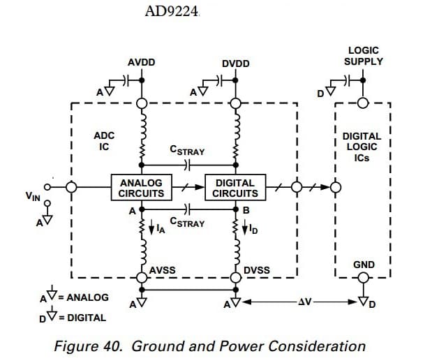
The main essence of the land division process is that the return currents of the “noisy” digital or power parts of the circuit do not flow together with the return currents of the sensitive circuits: otherwise, the sensitive circuits can detect fluctuations in the voltage of noise on the ground polygons and interpret them as part of a useful signal, which will inevitably lead to errors in operation.
To do this, two chains with different names are created in the project (for example, A_GND and D_GND). Sensitive ground circuits are connected to A_GND, and “noisy” ones are connected to D_GND. But if digital and analog blocks communicate with each other (and this happens almost always), you need to connect the a_gnd and D_GND circuits to each other (otherwise, there will be no place for return currents to flow).
How to do this correctly? There are different opinions on this point. I usually connect these circuits to each other with a zero resistor, placing it near the power source on the circuit Board.
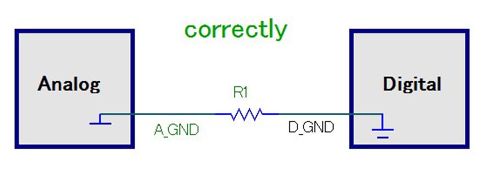
If you work in Altium Designer, a special type of component called Net Tie is provided for this purpose, and you can use It as well.
Sometimes it is recommended to use inductance to connect these earth circuits, arguing that it blocks high-frequency interference well. But I strongly advise you not to do this: do not forget that the return currents of signals between the digital and analog parts of the circuit will flow through this inductance. This will lead to a strong distortion of the signal form and, possibly, to a complete failure of the circuit. Inductors are useful to use in power circuits to filter it, but you also need to do this carefully. Let’s look at this question in a little more detail.
First of all, you need to remember one simple rule: the inductance of the filter must always be paired with the capacitor. The circuit without a capacitor, most likely, will not work at all. Why? See the first section of this article.

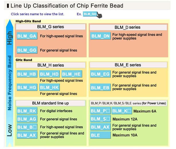
The type and value of inductance is selected based on the expected power interference intensity, the interference spectrum, and the characteristics of your circuit. Of course, the current reserve must be observed. In my practice, I often use inductors of the BLM series from Murata for power filtering: they are designed specifically for filtering interference in various types of equipment. A brief description of the inductors of the BLM series is shown in the figure.
9. Consider transients
Transients – this is how the system behaves before the onset of the steady state. In particular, transients can be understood as power-on moments, moments when the load is connected to the source, key switching, and much more. In General, a detailed discussion of transients is a topic for a whole series of articles. In this article, we will consider in more detail the issue of power-up, as occurring most often.
Situation 1. You have connected a circuit Board with wires to a laboratory power supply. You supply power and find that your Board, instead of starting, is in a cyclic reboot mode. What is happening and what should to do?
Indeed, such situations can occur and the reason is in the transition process. At the time of start-up, your Board may consume several times more current than at the time of regular operation. This is especially noticeable if there is a powerful processor on the Board.
An increasing pulse of current passes from the power source to the Board through the wires, which, unfortunately, are not perfect: they have both parasitic resistance and parasitic inductance. All this leads to a failure of the voltage on the Board: this failure works out the processor supervisor and as a result we have a cyclic reboot. There are several solutions to the problem: shorten the wires and increase their cross-section area, use laboratory power sources with feedback, or even put a power Converter on the Board and supply a higher voltage to the Board.
Situation 2. You supply power to your Board and then notice that at the initial moment, for some reason, the led winks slightly, which should be turned off. Or for a short moment, some power Converter starts working, which, like, should be blocked in the processor SOFTWARE. Or the relay clicks randomly.
What is it? Error in the code? Everything can be simpler and more complex at the same time. It is possible that you simply did not take into account the state of the processor’s I / o ports (or some other chip) at the time of reset and initial initialization. Meanwhile, this is an important parameter that should not be forgotten. Usually such moments are written in the documentation.
For example, STMicroelectronics explicitly States in the documentation for its stm32f750 microcontroller that all legs, except those responsible for programming and debugging, are configured as inputs during the reset and immediately after it, not pulled up to power or to the ground.
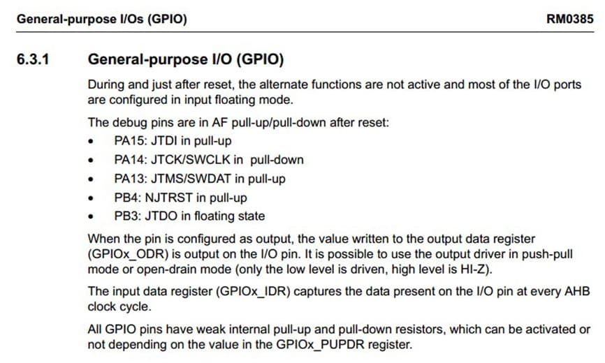
What does this mean for us? A track on a printed circuit Board with high – impedance inputs on both sides is an excellent antenna for detecting all kinds of interference. And if she wound up, for example, the EN input of any power, or controls the relay, the bootstrap moments, this power supply can randomly turn on and off and relays are clicking with insane speed literally at your fingertipsFortunately, this problem is solved quite simply: it is enough to put pull-up resistors to GND or VCC with a nominal value of 10 … 100 kOhm on critical circuits. They reliably record the signal strength at the moment of initialization and prevent chaotic switching of peripherals.
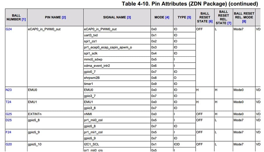
However, it is worth remembering that the state of the chip pins at the time of reset and initial initialization is very individual and depends on the specific chip. And if in the same STM everything is quite simple and clear, then, for example, in the AM4376 processor from Texas Instruments everything is much trickier: part of the GPIO has a HIGH-Z state, some have PU suspenders, others PD:
Situation 3. You have completely de-energized your Board, but the led continues to burn on it, or are the chips showing some activity? What is it, a perpetual motion machine? Unfortunately, everything is much simpler. Most likely, you still have some USB-UART Converter or other peripherals connected to the Board that are powered on the side and have a high logical level on their pins. The fact is that any chip has two diodes on its inputs, switched between GND and VCC. Through these diodes, the voltage from the input of the chip can penetrate to the power output of the chip and then spread throughout the Board, as shown in the figure.
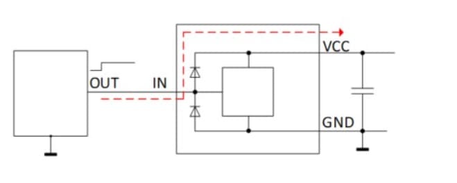
Of course, it is unlikely to fully power the entire Board in this way. However, some intermediate voltage level can be formed on the VCC circuit: less than the supply voltage of the chip, but still sufficient to make the chips appear in an “incomprehensible” state. Fortunately, most chips are still not particularly sensitive to such voltage flows, but this problem should not be forgotten, and if necessary, you should put special isolation buffers in critical circuits.
Well, now we have the last paragraph of this article.
10. Read the documentation for the components used
It does contain answers to most of the questions, including those that we have discussed in this article. Yes, sometimes this documentation contains tens, hundreds or even thousands of pages, but the time spent on studying them at the design stage of the device will more than pay off during the product launch and debugging.
Study the schema on debug Board provided by the manufacturer, and also overlook examples of topology of printed circuit boards: it is usually best producer no one will tell you how to tie the chip and dissolve it under the PCB. Do not forget about Errata, there are sometimes hidden surprises. Always try to understand what each leg is doing in the chip you are using: not connected properly can ruin all the work.
Conclusion
In this article, we have reviewed ten basic rules for designing electrical circuits. I hope this will help novice developers avoid at least the simplest mistakes when designing schemes. And most importantly, develop devices and don’t be afraid to experiment, because practice is still the best teacher in the end.